Electronics
Electronics
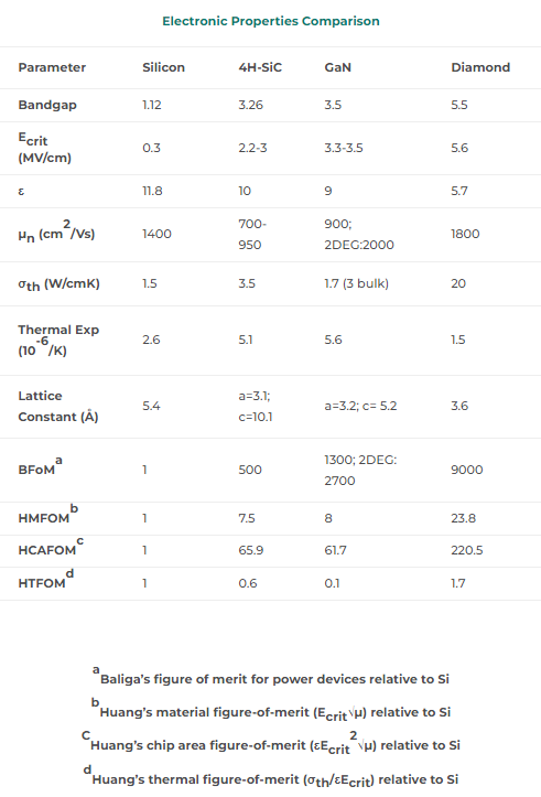
Wide Bandgap (WBG) semiconductors such as SiC and GaN have long been seen as the next fundamental step after silicon, specifically for high power and frequency devices. SiC and GaN are both somewhat mature with high quality substrates commercially available, although there is still a substantial amount of research being done on these materials. Diamond, however, has perhaps the most favorable material properties for use as a semiconductor including high thermal conductivity, high breakdown field, high bulk carrier mobility, low dielectric constant, high radiation tolerance, and the ability to operate at elevated temperatures. Furthermore, as shown ‘Electronic Properties Comparison’ table below, diamond excels over other prominent materials making it the ideal electronic device material for both active (high-frequency field-effect transistors (FETs) and high-power switches) and passive devices (Schottky diodes).
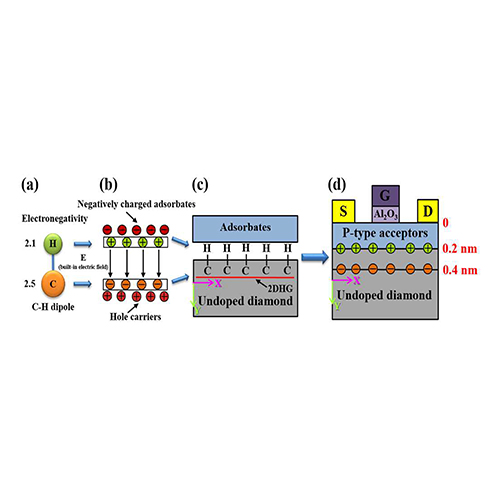
Gem industry that has popularized diamond as a fashion symbol for a very long time has begun pioneering new fabrication technologies for diamond to be used for a wide range of electronic and industrial applications. Heyaru Engineering is one of these companies making consistent advancements. Despite these rapidly advancing fabrication techniques, diamond still suffers from an asymmetrical doping complex in that p-type behavior (using boron) is much easier to obtain than the corresponding n-type behavior. While new techniques will inevitably be established in the next 5-10 years for creating n-type diamond, recent research has focused on the development of new architectures able to capitalize on existing diamond synthesis capabilities. The most promising approach appears to be two-dimensional hole gas (2DHG) field effect transistors which will also be the prime focus of our research.
(Illustration of the charge doping to induce a 2DHG channel for diamond FETs. (a) The carbon-hydrogen dipole formed during hydrogen termination, (b) Migration of charge in diamond by the negatively charged adsorbates (those with higher binding energies than the hydrogenated diamond surface), (c) formation of 2DHG, (d) Full diamond FET with source, drain, and gate.)
|
Electronic Properties Comparison |
||||
| Parameter | Silicon | 4H-SiC | GaN | Diamond |
| Bandgap | 1.12 | 3.26 | 3.5 | 5.5 |
| Ecrit (MV/cm) | 0.3 | 2.2-3 | 3.3-3.5 | 5.6 |
| ɛ | 11.8 | 10 | 9 | 5.7 |
| µn (cm2/Vs) | 1400 | 700-950 | 900; 2DEG:2000 | 1800 |
| σth (W/cmK) | 1.5 | 3.5 | 1.7 (3 bulk) | 20 |
| Thermal Exp (10-6/K) | 2.6 | 5.1 | 5.6 | 1.5 |
| Lattice Constant (Å) | 5.4 | a=3.1; c=10.1 | a=3.2; c= 5.2 | 3.6 |
| BFoMa | 1 | 500 | 1300; 2DEG: 2700 | 9000 |
| HMFOMb | 1 | 7.5 | 8 | 23.8 |
| HCAFOMc | 1 | 65.9 | 61.7 | 220.5 |
| HTFOMd | 1 | 0.6 | 0.1 | 1.7 |
|
aBaliga’s figure of merit for power devices relative to Si bHuang’s material figure-of-merit (Ecrit√µ) relative to Si CHuang’s chip area figure-of-merit (ɛEcrit2√µ) relative to Si dHuang’s thermal figure-of-merit (σth/ɛEcrit) relative to Si |
||||
Gem industry that has popularized diamond as a fashion symbol for a very long time has begun pioneering new fabrication technologies for diamond to be used for a wide range of electronic and industrial applications. Heyaru Engineering is one of these companies making consistent advancements. Despite these rapidly advancing fabrication techniques, diamond still suffers from an asymmetrical doping complex in that p-type behavior (using boron) is much easier to obtain than the corresponding n-type behavior. While new techniques will inevitably be established in the next 5-10 years for creating n-type diamond, recent research has focused on the development of new architectures able to capitalize on existing diamond synthesis capabilities. The most promising approach appears to be two-dimensional hole gas (2DHG) field effect transistors which will also be the prime focus of our research.
(Illustration of the charge doping to induce a 2DHG channel for diamond FETs. (a) The carbon-hydrogen dipole formed during hydrogen termination, (b) Migration of charge in diamond by the negatively charged adsorbates (those with higher binding energies than the hydrogenated diamond surface), (c) formation of 2DHG, (d) Full diamond FET with source, drain, and gate.)
The diamond surface is extremely unique in that it can be easily functionalized to change its electron affinity (EA: difference between the vacuum energy and the conduction band energy) and consequently also its ionization energy (IE: energy required to pull an electron out of diamond’s valence band). Hydrogen termination of the diamond surface has been consistently reported to demonstrate a negative EA (-1.3 eV) and comparably low IE of 4.2eV. Conversely, oxidation of the hydrogen terminated diamond states through ozone exposure has been shown to raise the EA to +1.7 eV and the IE to 7.2eV. The resulting reduced IE for a hydrogen terminated diamond surface allows electrons to readily transport into materials on the surface with higher binding energies. This process is known as surface transfer doping as the subsequent electron vacancies induce a highly conductive p-type layer just under the diamond surface which can function as a channel in a field effect transistor (FET).


